
Electronic Devices
Semiconductor Diode, Application of Junction Diode as a Rectifier
- A P-n junction can be formed during the crystal growth in a pure semi-conductor
- At the junction, the free electrons from n-region migrate towards p-region and the holes in p-region migrate towards n-region. This process is known as DIFFUSION
- Due to diffusion, positive ions are left over in n-region and negative ions are left over in P-region near the junction. These ions are immobile.
- Due to the immobile ions on either side of the junction an internal electric field in formed at the junction which is directed from n-region to p-region.
- Charge carrier region is not formed at p-n junction due to the combination of electrons and holes i.e called as DEPLETION LAYER.
- If V is the barrier potential and D is the thickness of the depletion layer, then the electric field intensity across the junction is \tt E=\frac{v}{d} from n side to p side.
- The direction of electric field is always from n-side to p-side.
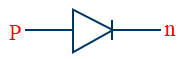
- Circuit symbol of p-n junction diode
- Due to the very small size of p-n junction diodes they are used in micro circuits.
- The movement of holes and electrons towards the junction and their recombination reduces the width of the charge depleted region.
- A.C resistance of the diode \tt R_{a.c}=\frac{\Delta v}{\Delta I}
- The Avalanche breakdown in reverse bias is due to the breaking of covalent bonds as a result of collision of electrons and holes with the valance electrons.
- Zener breakdown in reverse bias is due to the breaking of covalent bonds simultaneously.
- Light emitting diode (LED) is forward biased.
- LED are used as photo-luminescent panels in road signs, indicator lights etc.
Applications of Junction diode - Solar cells are used in calculators. Solar arrays generate electricity.
- Zener diode is a properly doped p-n junction diode which is operated in the breakdown region in reverse bias mode.
- Zener diode has a sharp breakdown voltage in the reverse bias condition. This voltage is called Zener Voltage (Vz).
- Silicon is preferred over germanium while constructing Zener diodes, due to its high thermal stability and current compatibility.
- More number of electron-hole pairs are created due to the strong electric field at the junction at Zener voltage, which increases the reverse current without change in voltage.
- Zener diode is used as a voltage regulator.
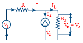
- \tt I_{L}=\frac{v_{o}}{R_{L}}=\frac{v_{z}}{R_{L}}=constant
- Voltage across series resistance,
V = input voltage – zener voltage, V = Vi – Vz - Current through series resistance (R)\tt I=\frac{v}{R}=\frac{v_{i}-v_{z}}{R}
- Current through Zener diode, IZ = I – IL
SemiConductor Diode View the Topic in this video From 00:24 To 4:54
View the Topic in this video From 00:27 To 10:31
Disclaimer: Compete.etutor.co may from time to time provide links to third party Internet sites under their respective fair use policy and it may from time to time provide materials from such third parties on this website. These third party sites and any third party materials are provided for viewers convenience and for non-commercial educational purpose only. Compete does not operate or control in any respect any information, products or services available on these third party sites. Compete.etutor.co makes no representations whatsoever concerning the content of these sites and the fact that compete.etutor.co has provided a link to such sites is NOT an endorsement, authorization, sponsorship, or affiliation by compete.etutor.co with respect to such sites, its services, the products displayed, its owners, or its providers.
1. dc Current Gain
It is defined as the ratio of the collector current (IC) to the base current (IB).
\beta_{dc} = \frac{I_{C}}{I_{B}}
2. ac Current Gain
It is defined as ratio of change in collector current (ΔIC) to the change in base current (ΔIB).
\beta_{ac} = \frac{\Delta I_{C}}{\Delta I_{B}}
3. Voltage Gain
It is defined as the ratio of output voltage to the input voltage.
A_{v} = \frac{V_{0}}{V_{i}} = -\beta_{ac} \times \frac{R_{0}}{R_{i}}